Samsung Electronics Co., Ltd., the world leader in advanced memory technology, today introduced a blueprint for next-generation flash memory solutions that will meet the ever-increasing demands of big data networks, cloud computing and real-time analysis.
At Flash Memory Summit 2016*, held in the Santa Clara (CA) Convention Center, Samsung showcased its 4th generation Vertical NAND (V-NAND) and a line-up of high-performance, high-capacity solid state drives (SSDs) available for its enterprise customers as well as Z-SSD, a new solution providing breakthrough performance for flash-based storage.
Samsung’s new flash storage devices are expected to contribute significantly to the global IT industry in meeting the growing storage requirements of today’s enterprise computing environment. These solutions will accommodate enormous amounts of data, and extremely high-speed information processing, while enhancing the total cost of ownership (TCO) for data centers.
“With our 4th generation V-NAND technology, we can provide leading-edge differentiated values in high capacity, high performance and compact product dimensions, which together will contribute to our customers achieving better TCO results,” said Young-Hyun Jun, President of the Memory Business at Samsung Electronics. “We will continue to introduce more advanced V-NAND solutions and expand our flash business initiatives in maximizing an unbeatable combination of performance and value.”
Samsung’s 4th Generation V-NAND stacks 30 percent more layers of cell-arrays than its predecessor
Samsung introduced its 4th generation, 64-layer triple-level-cell V-NAND flash memory that pushes the envelope of NAND scaling, performance and storage capacity. Stacking 64 layers of cell-arrays, the new V-NAND can increase its single-die density to an industry-leading 512Gb and its IO speed to 800Mbps, which further distinguishes Samsung’s technology leadership in three-dimensional NAND cell structure design and production. Starting in August 2013, Samsung has previously introduced three generations of “industry-first” V-NAND products with 24, 32 and 48-layer vertical cell-array stacking technologies.
Samsung plans to provide the world’s first 4th generation V-NAND flash memory products in the fourth quarter of this year, which will help manufacturers to produce faster, more stylish and portable computing devices, while offering consumers a more responsive computing environment.
World largest capacity drive − 32TB SAS SSD − for enterprise storage systems

Samsung’s latest Serial Attached SCSI (SAS) SSD is the world largest single drive ever introduced to the industry based on 512-gigabit (Gb) V-NAND chips. A total of 512 V-NAND chips are stacked in 16 layers to form a 1-terabyte (TB) package and the 32-terabyte (TB) SSD contains 32 of those packages.
By adopting a new 4th generation V-NAND design, the 32TB SAS SSD can reduce system space requirements up to 40 times compared with the same type of system using two racks of hard disk drives (HDDs). The 32TB SAS SSD will come in a 2-5-inch form factor and be produced in 2017. Samsung also expects that SSDs with more than 100TB of storage capacity will be available by 2020, thanks to continued refinement of V-NAND technology.
1TB memory in a single BGA package

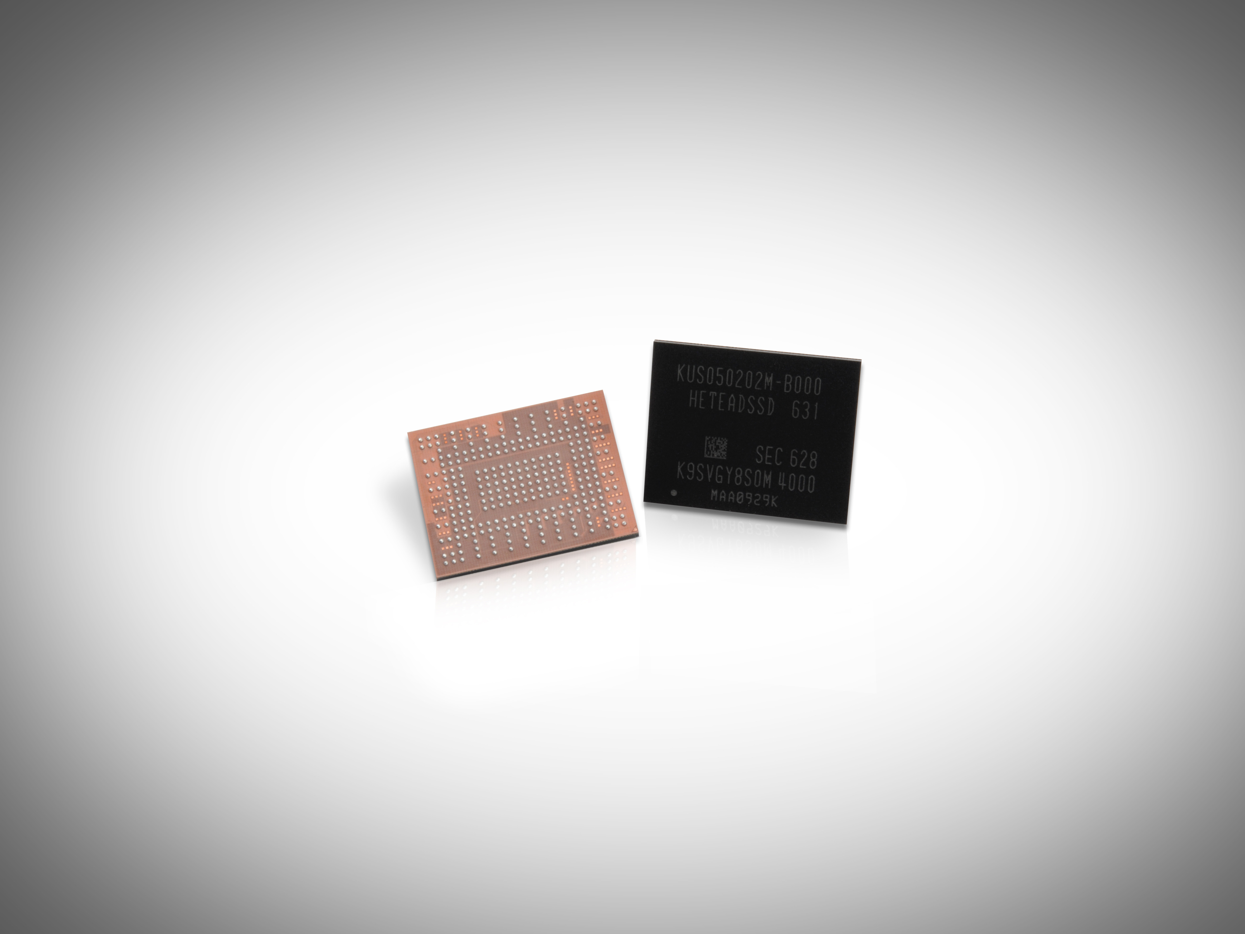
The Samsung 1TB BGA SSD features an extremely compact, ball grid array (BGA) package design that contains all essential SSD components including triple-level-cell V-NAND flash chips, LPDDR4 mobile DRAM and a state-of-the-art Samsung controller.
It will deliver unprecedented performance, reading sequentially at 1,500MB/s and writing sequentially at 900MB/s. By reducing its size up to 50 percent compared to its predecessor, the SSD weighs only about one gram (less than half the weight of a U.S. dime), making it ideal for ultra-compact next generation notebooks, tablets and convertibles.
Next year, Samsung plans to launch its 1TB BGA SSD by adopting a high-density packaging technology called “FO-PLP (Fan-out Panel Level Packaging)” which Samsung Electronics developed with Samsung Electro-Mechanics.
New ‘Z- SSD’ breaks through performance limits of current NAND flash memory storage

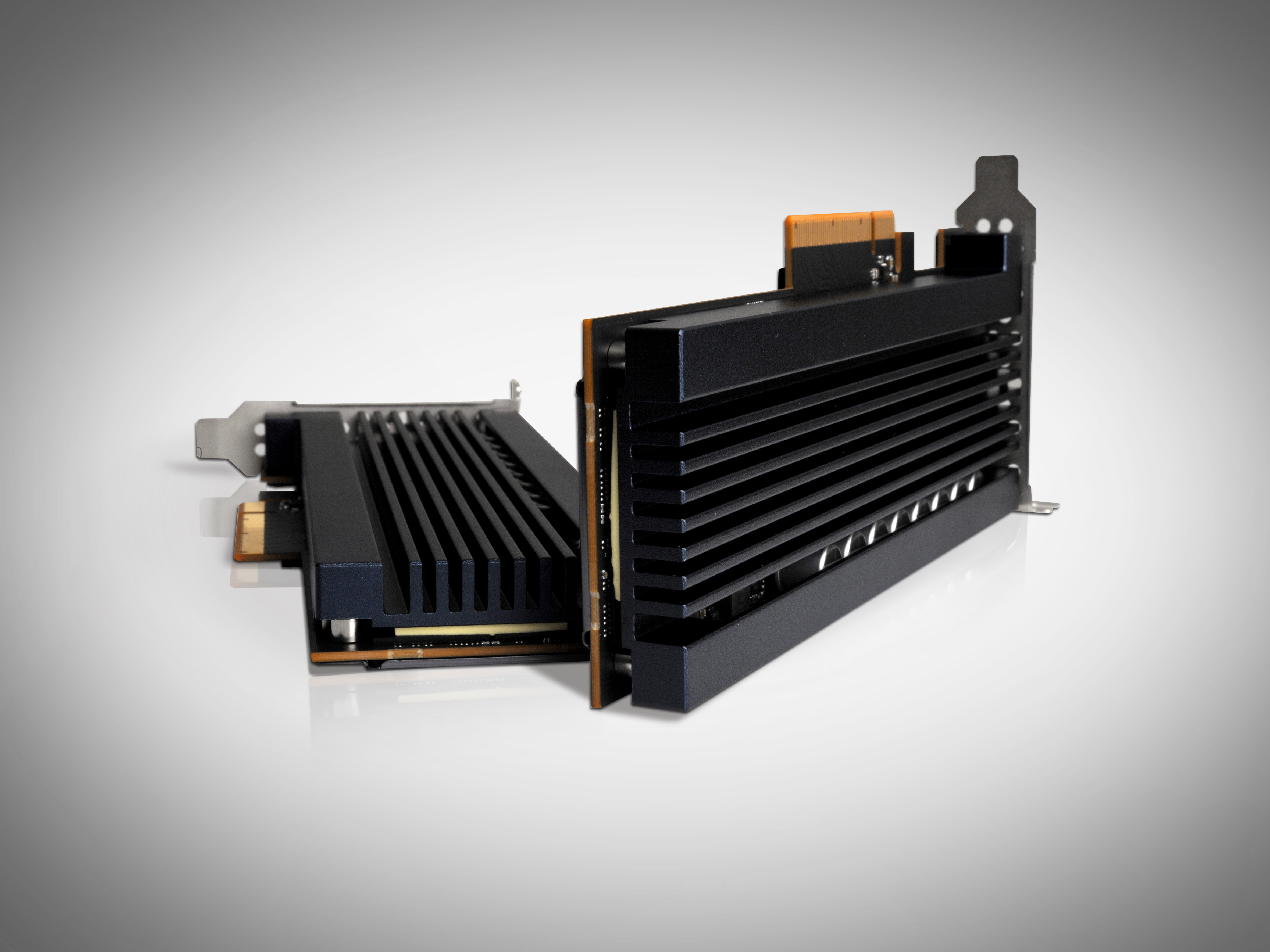
Samsung has also developed a high performance, ultra-low latency SSD solution, the Z-SSD. Samsung’s Z-SSD shares the fundamental structure of V-NAND and has a unique circuit design and controller that can maximize performance, with four times faster latency and 1.6 times better sequential reading than the Samsung PM963 NVMe** SSD.
The Z-SSD will be used in systems that deal with extremely intensive real-time analysis as well as extending high performance to all types of workloads. It is expected to be released next year.

Recent Comments